

Specialty Gases
Hexachlorodisilane
Hexachlorodisilane (HCDS) is an important precursor in the semiconductor, fiber optics, and photovoltaic industries. HCDS is used as a semiconductor precursor in both atomic layer deposition (ALD) and chemical vapor deposition (CVD) methods. HCDS is used for low-temperature deposition of thin layers of epitaxial silicon and silicon oxynitride (SiNxOy) in semiconductor manufacturing. It is also an important precursor for silicon nitride (SiyNx) deposition using ALD.
AMS has a long-term supply agreement to provide ultra-high purity HCDS to end users through an exclusive partner. Interested parties can purchase HCDS via this partnership.


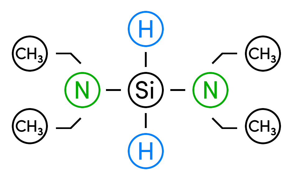
Aminosilanes
Traditionally, using chemical vapor deposition, a silicon gas such as dichlorosilane is co-fed into a tool with ammonia gas to produce a silicon nitride layer in the integrated circuit stack.
The latest technologies combine the amine with the silicon into a single aminosilane molecule. Aminosilanes can be deposited as silicon nitride layers at much lower temperatures and used in advanced tools such as atomic layer deposition (ALD).
Aminosilanes are synthesized by reacting chlorosilanes with an amine functional group. Utilizing this method, a diverse range of aminosilane molecules can be produced, but only a handful eventually realize commercial applications. AMS has direct experience with the production of various aminosilanes and understands the challenges associated with their production and purification.
AMS’s knowledge of chlorosilane precursors results in significant reductions in the cost of producing aminosilanes such as BDEAS and BTBAS. AMS reduces production costs while at the same time maximizing purity by optimizing the raw material chlorosilane costs.
AMS enables our clients to achieve best in class production costs by matching chlorosilane raw material supply to synthesis and purification technologies.
Bis(diethyl amino)silane
BDEAS

Bis(tertiary butyl amino)silane
BTBAS
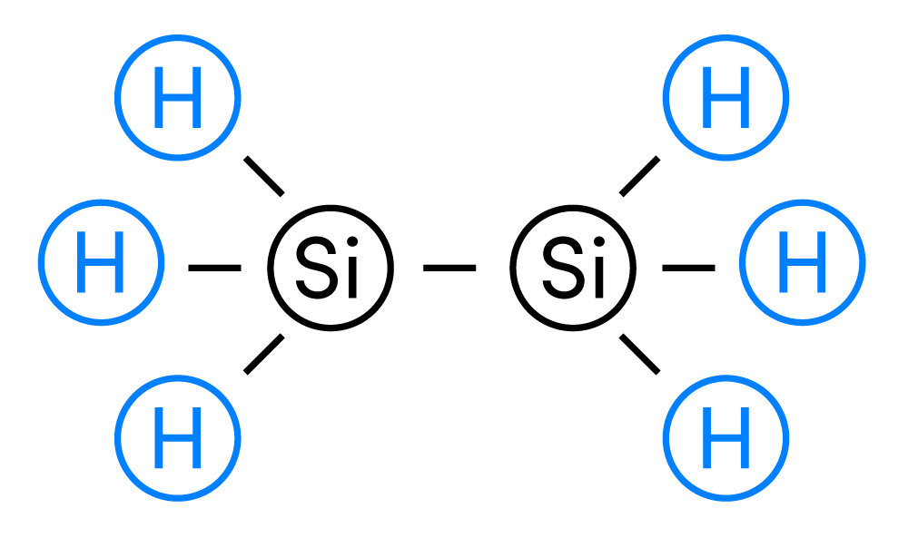
Disilane
Historically, disilane was produced in the hydrolysis of magnesium silicide as a byproduct of silane manufacturing. However, most commercial producers now synthesize disilane via pyrolysis of silane (SiH4). This synthesis method proceeds according to the chemical equation shown below:
Disilane is primarily used in the latest and most sophisticated generation of integrated circuits such as NAND Flash memory. It deposits at a lower temperature than silane enabling its use in smaller IC’s with a thermal budget constraint. Disilane can also be reacted with germanium in deposition tools to produce SiGe layers that strain the silicon and improve the performance of single-digit nano scale integrated circuits (ICs).
| DISILANE | |||
|---|---|---|---|
| Gas | Tool | Thin film | Application |
| Si2H6 | LPCVD | Micro polysilicon | Floating gate transistor |
| GeH4 | ALD/LPCVD | SiGe | Strain inducing layer CMOS |
Depending on the customer’s needs, the scope of AMS’s commercial offering can range from basic engineering packages to complete turnkey manufacturing systems. Our solutions are tailored for clients to gain successful market entry and allow for future expansion.
R&D
AMS is very experienced in commercializing new technologies, equipment, and production processes.
Our active research programs cover:
Materials and corrosion testing
Synthesis of new molecules
Analytical method development
Purification technologies.
AMS has the capability to test formation conditions for dozens of silicon precursors, including chlorosilanes, silanes and methyl chlorosilanes in our synthesis lab. With a range of equipment, we can test at conditions ranging -80°C to over 700°C and at pressures exceeding 30 bar(g).
AMS uses state-of-the-art analytical instruments for trace impurity analysis, including gas chromatography and mass spectrometry.


AMS employees have led development efforts resulting in successful commercialization of various equipment and technologies. We have expertise in all phases of technology development including bench-scale experimentation, theoretical modeling, prototyping, pilot testing, scale-up and commercialization. Example of commercial successes include:
Development of process to manufacture trichlorosilane via hydrochlorination. This process was successfully licensed and is being utilized by a majority of the largest polysilicon producers.
Continuous development of TCS production technology leading to design and installation of largest single train TCS production unit in the world.
Design and supply of CVD reactors for electronic grade silicon production. Previously enabled entry of first new producer to this market.
Developed and demonstrated the highest capacity commercially available STC hydrogenation reactor (STC converter).
Provided low emissivity coatings for over 100 CVD reactors.
This innovative development has led to over 20 patents in a wide array of high purity silicon and silicon gas production applications.
